

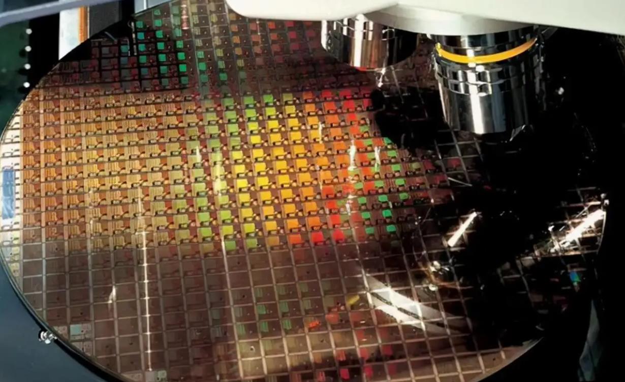
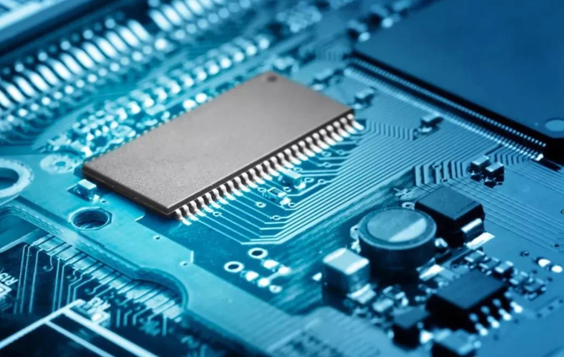
Semiconductor silicon wafer
In the field of IC chip manufacturing, plasma treatment technology has become an irreplaceable mature process, whether in chip source ion injection, crystal element coating, or our low-temperature plasma surface treatment equipment can achieve: removal of oxide film, organic matter, mask and other ultra-purification treatment on the surface of the crystal and surface activation to improve the surface wettability of the crystal.
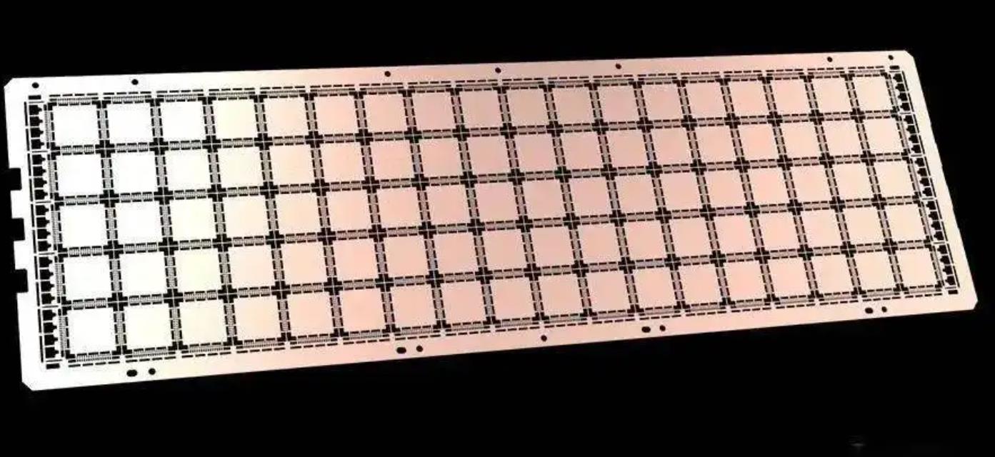
Surface treatment of lead frame
In the field of microelectronics packaging, the lead frame is used in the form of plastic sealing, which still accounts for more than 80%. It mainly uses copper alloy materials with good thermal conductivity, electrical conductivity and processing performance as the lead frame. Copper oxides and some other organic pollutants will cause the layering of sealing molding and copper lead frame, resulting in poor sealing performance and chronic gas infiltration after packaging. At the same time, it also affects the bonding quality of the chip and the bonding quality of the lead wire. Ensuring the ultra-clean lead frame is the key to ensure the reliability and yield of packaging. The plasma treatment can achieve the effect of ultra-purification and activation of the surface of the lead wire frame.
COB/COG/COF
With the rapid development of smart phones, people have higher and higher requirements for mobile phone camera pixels. Nowadays, the mobile phone camera module pixels manufactured by traditional CSP packaging technology cannot meet people's needs, while the mobile phone camera module manufactured by COB/COG/COF packaging technology has been widely used in the current mobile phone with 10 million pixels. But the yield of its manufacturing due to its process characteristics is often only about 85%, and the mobile phone yield is not high mainly because the centrifugal cleaning machine and ultrasonic cleaning can not do high cleanliness cleaning holder and Pad surface pollutants, resulting in holder and IR adhesion is not high and bonding poor problem, After plasma treatment, the organic pollutants and activated substrate on the holder can be ultra-clean removed, so that the adhesion between the holder and IR can be increased by 2-3 times. Also, the oxide on the Pad surface can be removed and the surface coarser, which greatly improves the success rate of banding.
- 在線咨詢
- 微信咨詢

微信掃碼咨詢
- Tel
- Phone0755-81452366
- Tel13510501616
- Top